ASRock Arc B570 Thermal Pads Guide
This is a guide to thermal pad thickness and a practice for me to write in markdown mode in Vim lol (But needless to say I cannot be held accountable if your B570 breaks).
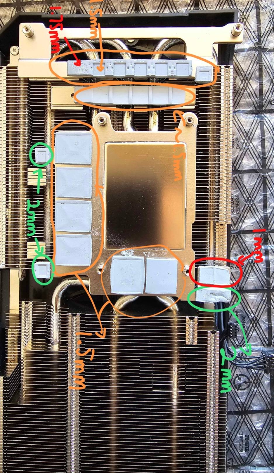
The interesting part: the heatsink has a thermal pad for a 5th VRAM chip that isn't on the board. ASRock probably reused the heatsink layout from the B580.
Measurement method
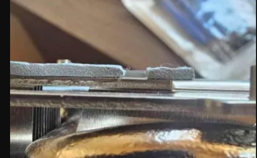
All thermal pad thicknesses were measured and rounded up to the nearest 0.25 mm, as pads compress under mounting pressure.
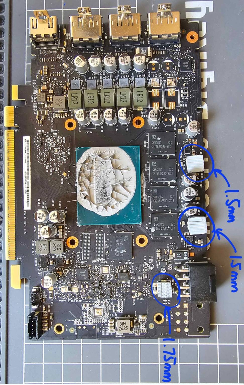
PCB side
There are 3 thermal pads contacting inductors on the PCB side, located near the top of the board (connector area).
- 2 at top side (memory VRM): 1.5mm
- 1 near 8-pin connector: 1.75mm
Heatsink side
- Memory: 1.5mm across
- Bottom memory VRM: 2mm (drMOS), 1mm (coils)
- Top memory VRM: 2mm (drMOS)
- Core VRM: 1.5mm (coils), 1.5mm (drMOS), ~1.75mm uncompressed observed
- Topside controller: 1.5mm
Comparison notes
Side-by-side comparison suggests the VRM drMOS pads are closer to 1.75mm uncompressed.
Notes
All of this is from measuring and eyeballing. How much a pad compresses depends on mounting pressure, the pad material, and heatsink tolerances.
I mostly wrote these down so I have them next time I repad or tear the card down.